-
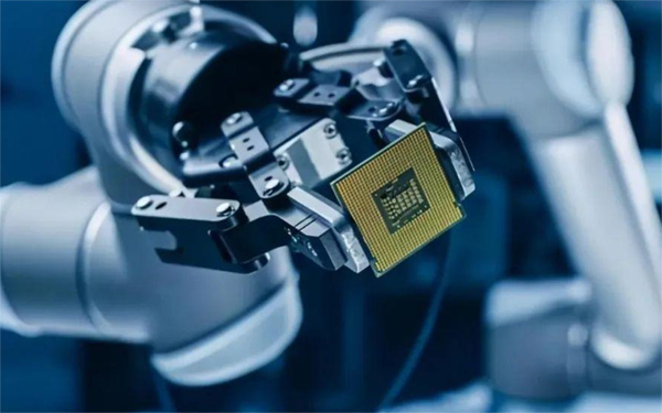
China successfully develops vacuum deposition machine, breaking Japan's technological monopoly
China has successfully overcome technological challenges and developed and mass-produced vacuum deposition machines, ending its long-term dependence on Japanese technology. This breakthrough means that the vacuum deposition machine, which was once priceless and in short supply, no longer needs to be controlled by others, breaking free from Japan's high price monopoly. But what exactly is a vacuum deposition machine? Why is it so important?
READ MOREVacuum deposition machine, in short, is an important instrument used for manufacturing screen panels, especially playing an indispensable role in the production of OLED screens. After it is started, the device can accurately heat the coating material in a vacuum environment, thereby improving the color performance and accuracy of the screen, ensuring a significant improvement in the overall quality of the screen panel.
OLED screens have become the mainstream choice for today's display screens, mobile phone screens, and computer screens. According to statistics, the demand for OLED screens in China has surged from 290 million pieces to 450 million pieces from 2019 to 2022. As a result, there is a huge demand for vacuum deposition equipment, which is indispensable for the production of OLED screens.
However, for a long time, we have been at the mercy of others in the field of vacuum deposition machines. This is mainly because the vacuum evaporation machine has extremely strict technical requirements, with a single vacuum production line stretching nearly a hundred meters. In addition, every production process must ensure the precision and accuracy of the products, which has become a technological bottleneck that China has not been able to overcome, leading us to rely on imports for a long time.
The core technology of vacuum deposition machines is mostly controlled by Canon in Japan, who often export their high-end vacuum deposition machines to countries such as the United States, the United Kingdom, and South Korea. This often means that even if China is willing to pay a high price, it can only purchase one or two machines in the end, which undoubtedly has a significant impact on Chinese companies such as Huawei and Xiaomi that have a large demand for OLED screens. In order to break through this technological bottleneck, China has begun to increase investment and research and development efforts in this field, in order to achieve independent technological breakthroughs.
Through the continuous efforts of all researchers, the Xinyihua team in China has finally broken through the key technologies of vacuum deposition machines such as alignment systems and evaporation sources, and successfully developed this equipment. Subsequently, companies such as Zhongshan Kaixuan and Hefei Laide also made significant progress, achieving large-scale production of vacuum deposition machines, thereby ensuring sufficient supply of OLED screens from domestic manufacturers. Prior to this, Japan's vacuum deposition machines had long dominated the global market, with high-end models even experiencing a shortage of supply and waiting in line.
Since the 1980s, Japan has been shifting its research focus to the field of liquid crystal displays, although at that time they were still beginners and lacked experience in this area. However, Japan's strength in research and innovation should not be underestimated. By learning LCD display technology from the United States and combining it with its own technological strength, Japan quickly conquered the core technology of OLED screens and even successfully developed a vacuum deposition machine capable of producing OLED screens.
Moreover, Japan has made significant achievements in OLED screen production technology, even surpassing its technology source, the United States. Until now, Apple Inc. still needs to import OLED screens for mobile phones from Japan, fully demonstrating Japan's leading position in this field. It is worth mentioning that Tokki, a subsidiary of Canon, is the only company in Japan that has mastered the technology of vacuum deposition machines. This company was founded by the father of Akihisa Tsugami in 1967 and was initially a relatively small company. Nowadays, although it has less than 350 employees, the number of vacuum evaporation machines produced each year is rare, with only a few, which makes the price of each equipment as high as 700 million yuan.
But even though there is a shortage of supply in the market, it is still difficult to obtain vacuum deposition machines. Canon has firmly established its dominant position in the international market with its monopoly on high-altitude vapor deposition technology. According to reports, Canon's vapor deposition machines have long held over 95% of the global market share, and despite producing less than a hundred units annually, they can generate profits of up to 5 billion yuan.
Although Tokki's vapor deposition machine is expensive, its excellent quality is beyond doubt. The OLED screens produced using its vapor deposition machine have vibrant colors and extremely high precision, making them the preferred choice for top companies such as Apple and Samsung. In fact, the high quality of Samsung mobile phone screens and the abundant production of OLED screens are inseparable from the strong support of Tokki vapor deposition machines. In addition, China's BOE Corporation attempted to acquire Tokki's vapor deposition machine for a high price of nearly 800 million yuan, but received a cold response from the other party. This not only demonstrates its confidence in not worrying about the sales market, but also reveals its attempt to curb China's rise in fields such as mobile phones and computers through its monopoly position.
Under the long-term monopoly of vacuum deposition machines in Japan, the production and development of OLED screens in China faced enormous challenges, and every step forward seemed difficult. However, the emergence of domestically produced vacuum deposition machines undoubtedly brings new hope to China in this field. So, compared to Japan's vacuum deposition machines, what level is our domestic equipment at? In fact, many Chinese companies have successively completed the research and development of vacuum evaporation machines, which not only fills the technological gap in the field of screens in China, but also breaks Japan's long-term monopoly in this field. This major breakthrough will undoubtedly bring profound economic benefits and social impact to our country.
Moreover, China's independently developed vapor deposition machine has the advantage of being a latecomer. For example, the K-200 vapor deposition machine invented by Zhongshan Kaixuan Technology Company not only integrates all the functions of Japanese vapor deposition machines, but also adds many innovative features to make it more attractive in the market. At the same time, the vapor deposition machines produced in China have achieved a coating accuracy of 1.5 microns, ranking among the world's leading. On the other hand, Canon in Japan has long lacked competitive pressure, and its equipment performance has remained stagnant, with a film coating accuracy of only 3 microns. In addition, the production efficiency of Canon in Japan is relatively low, and most components urgently need to be upgraded or replaced, otherwise they will face the risk of being caught up by China.
However, at the current stage of development, China's vacuum deposition machines are still in their infancy, and various technologies are not yet mature. Compared with Japan's deposition machines, there is still a certain gap. In addition, as our country's vapor deposition machine is a new product and has not yet taken a place in the world market, it will take time to open up the market and gain widespread recognition.
In fact, China is also facing similar challenges in the field of chips as vapor deposition machines, and has long been subject to foreign technological blockades. Among them, Huawei, a well-known domestic mobile phone brand, suffered significant losses due to chip issues, and the domestic public also felt helpless about this.
Although Huawei's Kirin chip is close to the most advanced 3nm technology in China in terms of design, and China has also entered the top five of the world's top ten manufacturers in the field of packaging and testing, demonstrating strong strength, there is still a gap of at least 20 years between China and the international leading level in chip manufacturing. In addition, due to export restrictions on advanced equipment from abroad, China's chip industry is facing many challenges in the short term, and the path to breakthrough remains difficult.
Various signs indicate that although China is rapidly developing in certain fields, it still faces many technological bottlenecks. Whether it is vapor deposition machines or chip manufacturing, and even more fields that are considered key technologies by foreign countries, China still has a long way to go. We must face up to these shortcomings and strive to overcome them.
072025.05
-
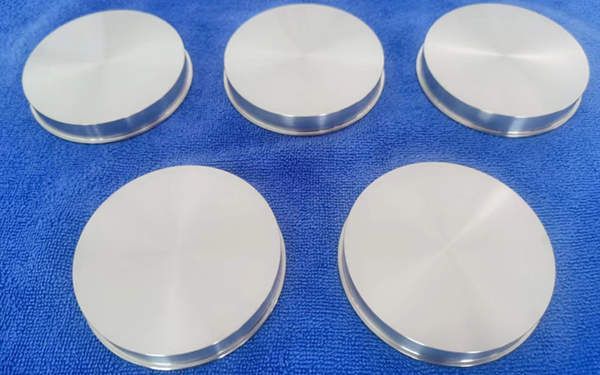
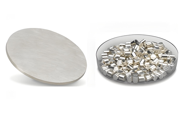
Comparison of Pure Metal Target Materials
The comparison of pure metal target materials can be analyzed in detail from the aspects of conductivity, thermal conductivity, corrosion resistance, mechanical properties, etc. The following is a comparison of several common pure metal target materials
READ MORECopper target material:
Conductivity and Thermal Conductivity: Copper target materials have the best conductivity and thermal conductivity, making them suitable for coating applications related to electrical and thermal management
Corrosion resistance: prone to oxidation in high temperature or humid environments, therefore not suitable for coatings sensitive to oxidation
Mechanical properties: relatively soft, easy to process, suitable for use in applications with high film uniformity requirements
Application areas: mainly used for electrical contact coatings, conductive films, integrated circuit interconnect layers, etc
Aluminum target material:
Conductivity and thermal conductivity: The conductivity and thermal conductivity are slightly inferior to copper, but the density is lower, making it suitable for application in electronic and optical thin films
Corrosion resistance: The naturally formed aluminum oxide layer is stable and corrosion-resistant, suitable for optical protective coatings or anti-oxidation applications
Mechanical properties: Medium strength, low density, suitable for thin films used in weight reduction design
Application areas: Reflective coatings, lightweight protective coatings, semiconductor wiring, etc
Titanium target material:
Conductivity and thermal conductivity: Low conductivity and thermal conductivity, but high mechanical strength and strong corrosion resistance
Corrosion resistance: Excellent corrosion resistance and oxidation stability, suitable for protective films in extreme environments
Mechanical properties: high strength, low density, suitable for hard coatings and structural coatings
Application areas: Hard coatings, corrosion-resistant films, biomedical coatings, etc
These pure metal target materials have their own advantages and disadvantages in terms of conductivity, thermal conductivity, corrosion resistance, and mechanical properties, and are suitable for different application scenarios.
072025.05
-
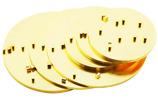
Introduction to Alloy Target Materials
Alloy target material is a material made by mixing two or more metal elements in a specific ratio, widely used in the field of thin film preparation. The composition and properties of alloy target materials can be adjusted according to specific application requirements to meet different application scenarios.
READ MOREAlloy target materials mainly include the following categories:
Iron cobalt target (FeCo): commonly used in the preparation of specific magnetic materials.
Aluminum silicon target (AlSi), titanium silicon target (TiSi), chromium silicon target (CrSi): used in semiconductor and integrated circuit manufacturing.
Nickel chromium target (NiCr), nickel aluminum target (NiAl), nickel vanadium target (NiV), nickel iron target (NiFe): suitable for various electronic and optoelectronic devices.
Titanium nickel target (TiNi): with shape memory effect, commonly used in special materials and equipment.
Rare earth target material: Utilizing the unique electronic structure of rare earth elements, it has important applications in display technology, data storage, and other fields.
072025.05
-
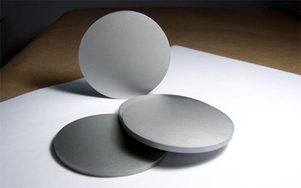
Types of ceramic target materials
These ceramic target materials are widely used in fields such as electronics, optics, aerospace, etc. due to their unique physical and chemical properties, meeting different application needs.
READ MOREOxide ceramic target material:
Transparent conductive oxides such as ITO (In ₂ O ∝) are used for touch panels and OLED anodes, while AZO (ZnO) is used for the TCO layer of thin-film solar cells. Other oxides such as Al ₂ O ∝, TiO ₂, PZT, and Fe ∝ O ₄ are used for optical coatings, anti reflective coatings, memory and magnetic recording media, etc.
Nitride ceramic target material:
Superhard nitrides: TiN is used for tool coatings and wear-resistant components, while AlN is used for semiconductor heat dissipation substrates. Optoelectronic nitrides, such as GaN, are used for LED epitaxy and RF devices. Superconducting nitrides, such as NbN, are used in superconducting quantum interference devices (SQUID).
Carbide/Boride Ceramic Target Material:
Superhard carbides: such as SiC used for nuclear reactor cladding materials and B ₄ C used for nuclear protection shielding. Conductive borides, such as TiB ₂, are used for electrode coatings and molten metal contact components.
Other ceramic target materials:
Fluorides, such as BaF ₂, CaF ₂, LiF, etc., are used in various optical and electronic applications.
Silicides such as CoSi ₂ and MoSi ₂ are used for high-temperature materials and electronic packaging.
Borides, such as HfB ₂ and TiB ₂, are used for high-temperature materials and wear-resistant coatings.
072025.05
-
Common vapor deposition materials and principles
Vacuum evaporation, abbreviated as evaporation, refers to the process of evaporating coating materials (or film materials) under vacuum conditions using a certain heating and evaporation method, causing them to vaporize and particles to fly to the surface of the substrate and condense into a film. Vapor deposition is an early and widely used vapor deposition technique, which has the advantages of simple film formation method, high film purity and density, unique film structure and performance.
READ MOREThe physical process of vapor deposition includes: evaporation or sublimation of deposited materials into gaseous particles → rapid transport of gaseous particles from the evaporation source to the substrate surface → adhesion of gaseous particles to the substrate surface to nucleate and grow into solid thin films → reconstruction or chemical bonding of thin film atoms.
Place the substrate in a vacuum chamber and heat the film material using methods such as resistance, electron beam, laser, etc., causing the film material to evaporate or sublime and vaporize into particles (atoms, molecules, or atomic clusters) with a certain energy (0.1-0.3 eV). Gaseous particles are rapidly transported to the substrate in a nearly collision free linear motion. Some of the particles that reach the surface of the substrate are reflected, while others are adsorbed onto the substrate and undergo surface diffusion. Two dimensional collisions occur between deposited atoms, forming clusters, and some may remain on the surface for a short period of time before evaporating. Particle clusters constantly collide with diffusing particles, either adsorbing or releasing single particles. This process is repeated, and when the number of aggregated particles exceeds a certain critical value, they become stable nuclei, which then continue to adsorb and diffuse particles and gradually grow. Finally, through the contact and merging of adjacent stable nuclei, a continuous thin film is formed.
The vacuum evaporation process generally includes steps such as substrate surface cleaning, preparation before coating, evaporation, component removal, post coating treatment, testing, and finished product.
072025.05